


High Precision JGS1 / JGS2 / JGS3 Optical Quartz Glass Plates & Substrates
(Double-Sided Optical Polished | 0.1mm–20mm Thickness | Deep UV to Far IR High Transmittance | Custom CNC Cutting)
1. Product Overview & Key Highlights
Our JGS1, JGS2, and JGS3 Optical Quartz Glass Substrates are precision-manufactured for high-end laser systems, UV/IR spectroscopy, semiconductor wafer fabrication, high-temperature sight glasses, and laboratory optical research.
Available in thicknesses from 0.1mm ultra-thin sheets up to 20mm heavy-duty blocks, all substrates undergo high-precision double-sided optical polishing (80/50, 60/40, or 40/20 scratch-dig) to achieve ultra-low surface roughness (Ra < 0.5 nm) and minimal wavefront distortion. We support full custom fabrication based on your CAD drawings (DXF, DWG, STEP, PDF), including custom shapes, precision holes, step-milled borders, and optical AR coatings.
Broad Spectral Transmission Range: High transparency across Deep UV (185nm), Visible, and Mid-to-Far Infrared (up to 3500nm).
Extreme Thermal Resistance: Continuous working temperature up to 1100°C, short-term thermal stability up to 1200°C–1300°C.
Near-Zero Thermal Expansion: Thermal expansion coefficient of only 5.5 x 10^-7 / K, offering exceptional thermal shock resistance (survives direct quenching from 1100°C into cold water).
Ultra-Low Surface Roughness: Double-sided polishing guarantees Ra < 0.5 nm and parallelism down to < 1 arcmin.
Chemical & Radiation Resistance: High chemical inertness against strong acids (except HF) and superior dielectric strength.
2. JGS1 vs. JGS2 vs. JGS3 Material Comparison Table
| Parameter / Grade | JGS1 (Synthetic Fused Silica) | JGS2 (Fused Quartz) | JGS3 (Infrared Fused Quartz) |
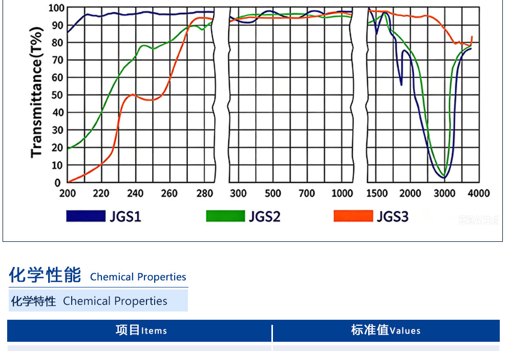
| Transmission Range | Deep UV to NIR (185 nm – 2500 nm) | UV to NIR (220 nm – 2500 nm) | VIS to Deep IR (260 nm – 3500 nm) |
| Typical Transmittance | ≥ 90% (at 200 nm), ≥ 92% (VIS) | ≥ 85% (at 220 nm), ≥ 90% (VIS) | ≥ 85% (at 2730 nm IR peak) |
| Bubble / Purity Class | Bubble-free (Class 0), Purity 99.999% | Class 1 / Class 2, Purity 99.99% | Class 1, OH content < 5 ppm |
| Thermal Expansion (CTE) | 5.5 × 10⁻⁷ / K | 5.5 × 10⁻⁷ / K | 5.5 × 10⁻⁷ / K |
| Max Working Temp | 1100°C (Continuous) / 1250°C (Short) | 1100°C (Continuous) / 1250°C (Short) | 1100°C (Continuous) / 1250°C (Short) |
| Primary Applications | Deep UV optics, laser windows, lithography | Standard optical windows, sight glasses | Infrared spectroscopy, thermal sensors |
3. General Technical Specifications
| Parameter | Standard Capability & Custom Range |
| Product Name | Optical Quartz Glass / Fused Silica Substrates |
| Grade Options | JGS1 (Far UV) / JGS2 (UV-Vis) / JGS3 (Infrared) |
| Thickness Range | 0.1 mm to 20.0 mm (e.g., 0.1mm, 0.2mm, 0.5mm, 1.0mm, 2.0mm, 3.0mm, 5.0mm, 10mm, 20mm) |
| Dimensional Tolerance | ± 0.05 mm to ± 0.1 mm (Precision CNC Cutting / Laser Dicing) |
| Thickness Tolerance | ± 0.05 mm to ± 0.1 mm (based on thickness) |
| Surface Quality (Scratch-Dig) | 60/40 (Standard Optical) / 40/20 (Precision Laser Grade) / 20/10 (High Precision) |
| Surface Flatness | Lambda / 4 to Lambda / 10 @ 632.8 nm |
| Surface Roughness (Ra) | < 0.5 nm (Super-Polished available upon request) |
| Parallelism | < 1 arcmin (up to < 10 arcsec) |
| Edge Processing | 45° Safety Chamfer, Polished Flat Edge, C-edge, R-edge |
| Max Working Temperature | Continuous: 1100°C |
| Thermal Expansion (CTE) | 5.5 x 10^-7 / °C (20°C–320°C) |
4. Typical Applications
Deep UV & Laser Optics (JGS1): Excimer laser optics (193nm, 248nm, 355nm), lithography photomask blanks, UV cure lamps, and spectrophotometer cuvettes.
Industrial & High-Temperature Sight Glass (JGS2): High-temperature furnace observation windows, semiconductor CVD/PVD chamber windows, UV sterilization lamp shields, and optical lenses.
Infrared & Thermal Sensing (JGS3): Mid-infrared sensor windows, pyroelectric thermal detectors, CO2 laser equipment observation windows, and IR spectroscopy cells.
Microfluidics & Bio-Chips: Microfluidic chip bonding, fluorescence microscopy coverslips, and electrophoresis plates
5. Frequently Asked Questions (FAQ)
Q1: How do I choose between JGS1, JGS2, and JGS3?
A:
Choose JGS1 if your working wavelength is in the Deep UV range (185nm–220nm) or requires minimal laser-induced fluorescence.
Choose JGS2 for standard UV, Visible, and Near-IR applications (220nm–2500nm) where high optical quality and cost-effectiveness are balanced.
Choose JGS3 if your application operates in the Infrared spectrum (up to 3500nm) and requires zero hydroxyl (-OH) absorption at 2730nm.
Q2: Can you manufacture ultra-thin quartz glass (e.g., 0.1mm–0.3mm)?
A: Yes. We specialize in precision thinning, lapping, and double-sided super-polishing of ultra-thin quartz sheets down to 0.1mm thickness with tight thickness uniformity and minimal edge chipping.
Q3: Can quartz glass be chemically tempered like regular float glass?
A: No. Pure quartz glass consists of almost 100% pure SiO2 and contains no alkali metal ions (like Na+ or K+), so it cannot undergo chemical ion-exchange tempering. However, quartz glass naturally possesses high mechanical strength, high hardness (Mohs 7), and superior thermal shock resistance.
Q4: What CAD file formats do you accept for custom shapes?
A: We accept standard 2D and 3D engineering CAD drawings including DXF, DWG, STEP, STP, IGES, and dimensioned PDF files.
6. Packaging Details & Global Safe Shipping
Class 1000 Cleanroom Packaging: Cleaned via multi-stage ultrasonic deionized water baths and packaged in dust-free cleanrooms.
Individual Optical Wafer / Gel Boxes: Small and ultra-thin substrates (0.1mm–1.0mm) are packed in dedicated dust-proof grid trays or vacuum wafer boxes to prevent friction.
Lens Tissue Interleaving: Thicker plates and custom blocks are interleaved with optical-grade, lint-free lens tissue and anti-static PE film.
Shockproof Moisture-Proof Outer Box: Sealed with multi-layer thick pearl cotton (EPE), bubble cushioning, and heavy-duty reinforced export cartons or wooden crates for zero-breakage international delivery.


